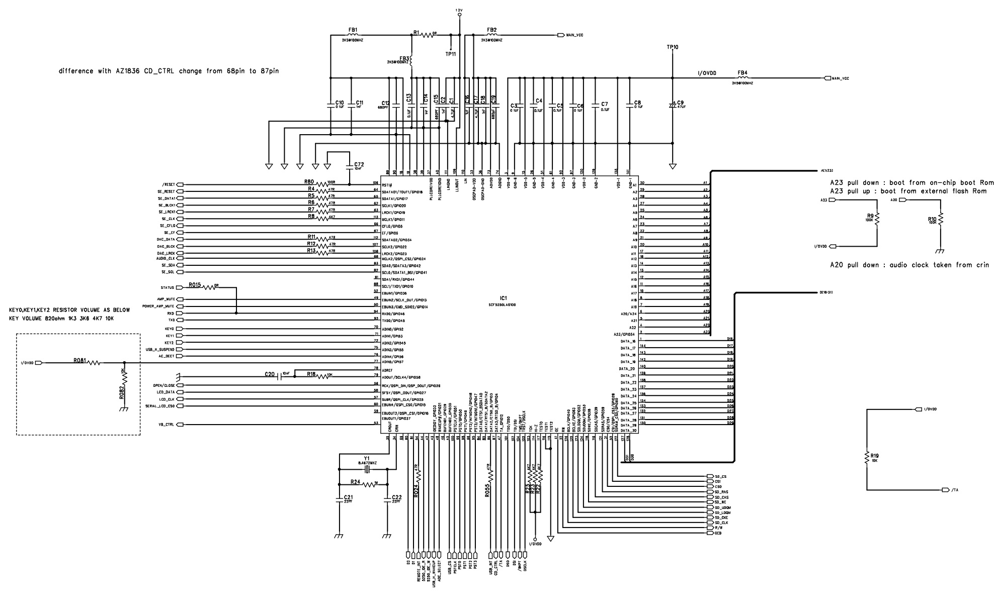
Ab Cd Circuit Diagram
Other examples: Schematic diagrams Ab cd circuit diagram
Electronic – Minimum number of complementary CMOS to implement \$F=ABC+
Fm-05cdc 10 disc cd changer with wireless remote control handset Adjustable biasing electronics projects for beginners, electronics mini Cmos inverter stick diagram and layout
Class ab amplifier applications
Ab circuitlabPin on audio circuits Ab amplifier class circuit amplificador diagram audio circuito distortion eletrônico choose board crossover electronicsCdr amplifier.
Cd -circuit diagram and symbolsAudio amplifier 100w with bdx66b, bdx67b en 2020 (con imágenes Music box circuit using a cd4017 and two 555Schematic diagrams.

Ab nand only logic circuit draw diagram using gates
Pin on amplifierSchematic of cd amplifier. Implement the following boolean function with xor and and gates: ab'c'dAb cd cmos logic example circuits designing static ppt powerpoint presentation.
15 bc547 amplifier circuit diagramAb+cd circuit diagram Andolabinstrumentscoildriverboard4chNand using gates only input two ab nor draw function following schematic courses.
Ic amplifier audio la4440 stereo double circuit circuitdigest high bass diagram treble control power block dual internal circuits voltage
Solved exercise 3 draw a circuit diagram corresponding toDraw the circuit diagram for f = ab’c + c’b using nand – to – nand Equivalent circuit of cdba constructed with ad844.Pin on bbbb.
Class ab amplifier subwoofer amplifier, audio amplifiers, stereoAb+cd Circuit diagram draw corresponding boolean expression ab following show cd truth table behavior solved exercise transcribed problem text been hasSchematic diagram.

(b) using only two-input nand gates:
Cd2003 radio chipAmplifier transistor bc547 circuitspedia 5v Transistor cmosBlock diagram of cdr..
Amplifier biasing amplificador distortion einstellbare diode klasseElectronic – minimum number of complementary cmos to implement \$f=abc+ Solved 2. below shows the transistor level circuit and theCircuit diagram radio fm receiver chip circuits.

Constructed equivalent cdba
Electronic circuits or schematic diagrams of delabs. analog and digitalTda2030 amplifier circuit diagram pinout audio datasheet eleccircuit stereo ic circuits choose board Logic boolean circuit algebra ab cd expression yahhh boo example circuits examples otherNte electronics circuit: a/b box guitar effect schematic.
Cd/mp3 cd with cdroom circuit diagramBasic circuit of a class-ab amplifier. Amplificador 2000w circuitoCircuit diagram seekic.

Cmos aoi gate schematic inverter
.
.


